| Location: Main >
Optical Crystals Ceramics > MgF2 GaAs InP Crystal Substrates > GAS-S100-R0508-0027D
|
|
|
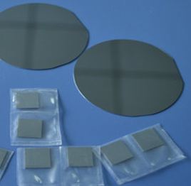
| Name: | DIA50.8xT0.275mm Crystal GaAs Wafer (100) DSP |
| P/N: | GAS-S100-R0508-0027D | | Keywords: | Dia50.8xT0.275mm,GaAs,(100),N-type,DSP,MOQ500pcs |
| Unit Price: |
S$66.00/pc
|
| Available: |
Call us
|
| Request: |
Add to Request List |
| Introduction: | GaAs(Gallium Arsenide) un-doped, Si-doped(N type) or Zn-doped(P-type) crystal substrates / wafers;
Single-surface polished or both-surface polished versions available
GaAs material as one of the new compound semiconductor materials that are most important and most widely used after silicon single crystal, features wide band gap, which gives it special properties for applications in optoelectronic, high-power and high-frequency devices. |
|
|
 |
|
Material: |
Single crystal GaAs, N-type |
|
Growth Method: |
VB/VGF |
|
Dopant: |
Si-doped (for N-type) (Note: contact us if P-type, that is Zn-doped, is expected) |
|
Carrier Concentration. |
0.5 ~ 4 x10E18 m^3 |
|
Etch Pit Density(EPD): |
<5000 cm^-2 |
| Resistivity: |
0.004 ~ 0.008 ohm.cm (with low resistivity) |
| Mobility: |
>1000 cm^2/v.sec. |
|
Flat Refernce: |
Primary/Secondary, as per SEMI EJ/US |
|
Outer Diameter: |
Dia 50.8, +/-0.2mm |
|
Thickness: |
275, +/-25um |
|
Surface Quality: |
40-20 S/D DSP (double-surface polished), with roughness Ra<5A |
|
TTV: |
10um max |
|
BOW: |
10um max |
|
WRAP: |
15um max |
|
Orientation: |
(100) ,+/-0.5 degrees
(100) 15 degrees off toward (111) +/-0.5 degrees |
|
Parallelism: |
<1 arc minute |
|
Chamfer: |
0.1 +/-0.05mm @ 45-deg |
|
Coating: |
Uncoated |
|
Packing: |
Vacuum packed; Std 25pcs/cassette |
|
MOQ: |
MOQ 500pcs per process | |
| |