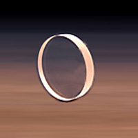
| Substrate Material: |
High purity UV fused silica (semiconductor std VIOSIL, used for photomask substrate) |
| Outer Diameter: |
67.0,-0.5/+0.0mm |
| Thickness: |
12.0, +/-0.2mm |
| Surface Quality: |
Double side polished (40-20 scratch and dig, MIL Standard) |
| Surface Flatness: |
<Lambda/10 @ 632.8nm over 25mm area on two surfaces over clear aperture |
| Parallemism: |
<1 arc minute |
| Clear Aperture |
>90% of outer diameter |
| Edge Surface: |
1.0mm x 45-deg protection chamfer |
| Surface Coating: |
Double side, extra-low absortption full dielectric/high damage threshold AR coating @ 1064nm,R<0.2% @1064nm(0-deg AOI); High energy laser applications |
| Packing: |
1pc/pack (vacuum packed) | |


